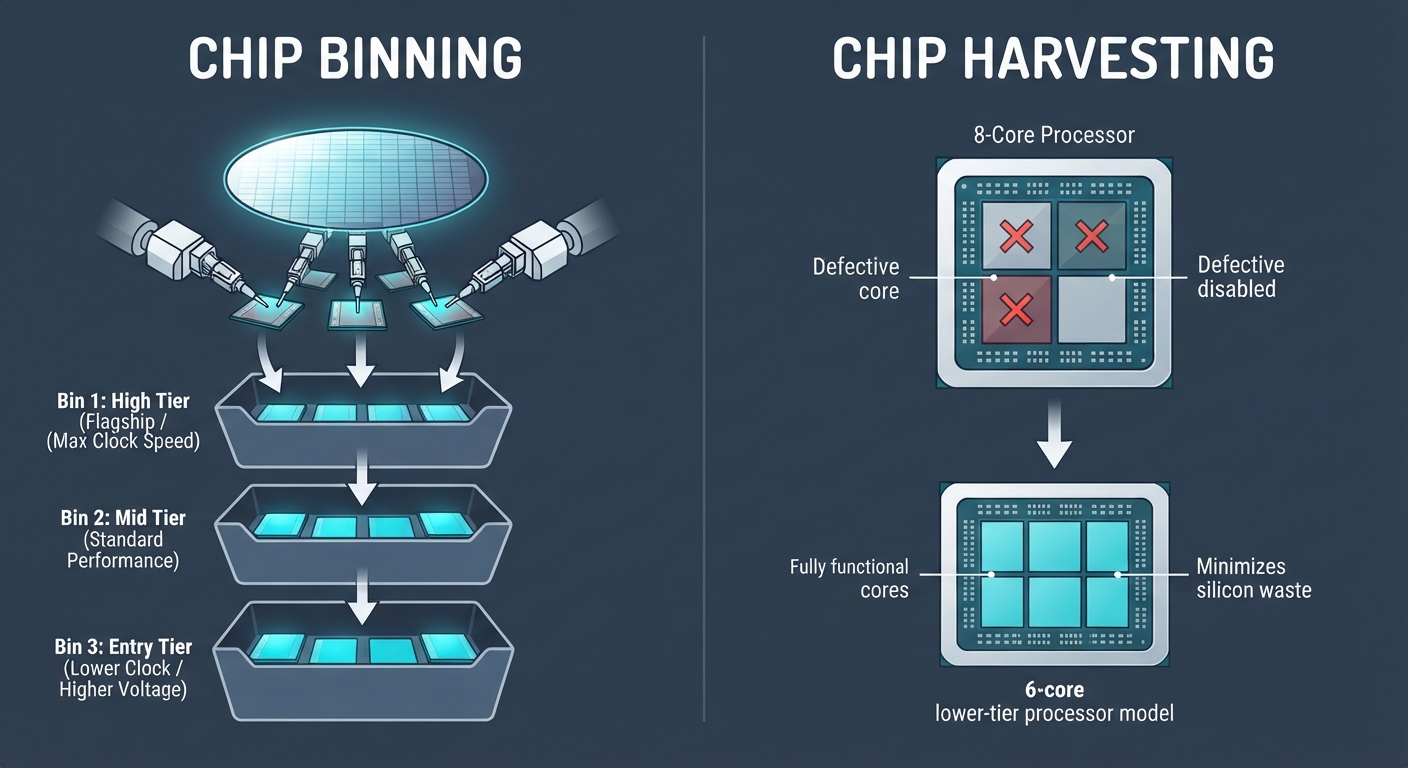
Chip Binning is the process of testing and sorting dies based on their actual performance (maximum stable clock speed, voltage requirements, and thermal output).
Chip Harvesting is the practice of salvaging a defective die by permanently disabling the broken portions to create a lower-tier product.
Chip binning
Chip binning is the industrial process of sorting and classifying microchips (such as CPUs, GPUs, and RAM) after they are manufactured, based on their actual performance and functional characteristics.
Because of the extreme precision required to build a processor—where billions of transistors are etched onto silicon at the nanometer scale—no two chips are truly identical, even if they come from the same silicon wafer. Binning allows manufacturers to turn these inevitable variations into a tiered product line.
1. Why Binning is Necessary: Manufacturing Variance
Ideally, every chip on a wafer would perform exactly as designed. In reality, microscopic inconsistencies occur during the fabrication process:
- Chemical Impurities: Tiny variations in the purity of the silicon.
- Lithography Deviations: Slight misalignments or variations in how the circuit patterns are projected.
- Thermal Gradients: Small differences in temperature across the wafer during production.
These variances mean that some chips are “perfect,” some are “mostly functional,” and some are “complete failures.”
2. How the Process Works
Once a wafer is sliced into individual dies, each chip undergoes a battery of tests. The results determine which “bin” the chip is placed into.
Testing & Sorting
- Functional Testing: Does the chip actually work? Do all the cores run? Is the integrated graphics functional?
- Speed Testing (Clock Frequency): At what frequency can the chip operate stably before it crashes or consumes too much power?
- Voltage/Power Testing: How much voltage is required to reach a specific speed? (Chips that require less voltage are more power-efficient and run cooler).
Hard vs. Soft Bins
- Hard Bins: These are coarse, physical categories (e.g., “Pass,” “Fail,” “Retest”) that often correspond to actual physical sorting trays in the factory.
- Soft Bins: These are digital records of why a chip failed or which specific performance tier it hit. Manufacturers use soft-bin data to analyze “yield” and improve the manufacturing process.
3. Strategies of Binning
Manufacturers use binning to maximize the amount of usable silicon from every wafer, a concept known as increasing the yield.
- Speed Binning: If a chip can stably hit 5.2 GHz, it is binned as a flagship (e.g., an Intel “K” series or AMD “X” series). If it can only stably hit 4.5 GHz, it is binned as a mainstream model.
- Core Harvesting (Core Disabling): If a design has 16 cores, but 2 of them are defective, the manufacturer doesn’t throw the whole chip away. Instead, they permanently disable the broken cores (via “laser cutting” or software locks) and sell it as a 14-core or 12-core processor.
- Feature Disabling: If the CPU cores are perfect but the integrated GPU is broken, the chip is binned as a “GPU-less” model (e.g., Intel’s “F” series).
- Power Tiers: Chips that are exceptionally power-efficient are binned for laptops or low-power desktops (e.g., Intel’s “T” series), where thermal limits are strict.
4. The Impact on the Consumer
Product Tiers and Pricing
Binning allows a company to sell one physical design as multiple different products. This creates a price ladder (Budget → Mid-range → Enthusiast) without having to design and manufacture entirely different chips for each level.
The “Silicon Lottery”
Because manufacturers must be conservative to ensure stability for all customers, they often bin chips lower than their actual potential. This leads to the “Silicon Lottery”:
- Golden Sample: You buy a mid-range chip, but you happen to get one that was actually high-quality silicon but was binned conservatively. These chips can often be overclocked significantly higher than others of the same model.
- Average Sample: The chip performs exactly as advertised.
- Poor Sample: The chip barely hits its rated speed and requires more voltage to stay stable.
Summary Table
| Feature | High-Bin (Flagship) | Mid-Bin (Mainstream) | Low-Bin (Budget) |
|---|---|---|---|
| Clock Speed | Highest ↑ | Moderate | Lowest ↓ |
| Core Count | All cores active | Some cores disabled | Many cores disabled |
| Power Efficiency | Very high (best silicon) | Average | Lower |
| Price | Expensive | Moderate | Cheap |
| Yield Role | “The Cream of the Crop” | “Fully Functional” | “Recovered Silicon” |
Chip Harvesting
Chip Harvesting (also referred to as Core Harvesting or Die Harvesting) is a specific manufacturing strategy used in the semiconductor industry to recover value from “defective” silicon.
While binning is the general act of sorting chips by performance (speed/voltage), harvesting is the act of salvaging chips that have physical defects by disabling the broken portions and selling the remaining functional parts as a lower-tier product.
1. The Economic Driver: The “Yield” Problem
To understand harvesting, you must understand the cost of a silicon wafer. A single wafer for a modern 3nm or 5nm process costs tens of thousands of dollars to produce.
Manufacturing is a game of Yield—the percentage of the wafer that results in usable chips. Because the transistors are so small, a single speck of dust or a microscopic crystal flaw on the silicon can render a specific area of the chip useless.
- If a manufacturer threw away every chip that had even one defect, the yield would be incredibly low, and the cost per working chip would skyrocket.
- Harvesting turns a “failure” into a “lower-tier success.”
2. How the Harvesting Process Works
The process happens in three main stages:
A. Detection (The Wafer Map)
Immediately after fabrication, the wafer undergoes Wafer Sort testing. Probes test every single core, cache block, and memory controller on every die. If the test identifies a “dead” area (e.g., Core #4 doesn’t respond), that die is flagged.
B. Disabling (The “Cut”)
Once a defect is found, the manufacturer must ensure the broken part cannot be accessed by the end-user, as a broken core would cause the entire system to crash (Kernel Panic/BSOD). They do this through:
- Hard Fusing (Laser Cutting): Using a high-precision laser to physically burn through the microscopic wires (traces) connecting the defective core to the rest of the chip. This is permanent and irreversible.
- e-Fuses: Electronic fuses that can be “blown” by sending a high-voltage pulse through a specific circuit, permanently breaking the connection.
- Microcode/Firmware Locks: In some cases, the defect is handled via a software lock in the chip’s internal ROM, though physical fusing is preferred for security and stability.
C. Re-categorization (The SKU Shift)
The chip is now functionally a different product.
- Example: A chip designed as a 16-core flagship that has 2 broken cores is “harvested” and rebranded as a 12-core mid-range processor.
3. Real-World Examples
CPU Harvesting (Intel & AMD)
Modern CPUs are designed with “redundancy” in mind. If you look at the product stack of a CPU family, you will see a logical progression of core counts (e.g., i9 → i7 → i5).
- The i9 is typically the “perfect” die (all cores working).
- The i7 and i5 are often harvested dies. A chip that failed the i9 tests but has 8 perfectly healthy cores becomes an i7.
GPU Harvesting (NVIDIA & AMD)
GPU harvesting is even more common because GPUs have thousands of small “Compute Units” or “Streaming Multiprocessors.”
- An RTX 4090 uses the AD102 die.
- An RTX 4080 also uses the AD102 die, but it is a harvested version. NVIDIA disables a portion of the CUDA cores and memory controllers to create the 4080. This allows them to sell chips that weren’t “perfect” enough to be a 4090.
4. Harvesting vs. Binning: The Key Difference
People often confuse these two terms, but they represent different types of “sorting.”
| Feature | Chip Binning (Performance) | Chip Harvesting (Functionality) |
|---|---|---|
| Cause | Natural variance in silicon quality. | Physical defects/broken transistors. |
| Condition | The chip is $100\%$ functional. | The chip is Partially broken. |
| Action | Setting clock speeds and voltage. | Permanently disabling parts of the chip. |
| Goal | To find the fastest “Golden Samples.” | To prevent the chip from being trash. |
| Result | i9-14900K vs. i9-14900 (Non-K). | i9 (16-core) → i7 (8-core). |
The “Salvage” Logic
If you buy a mid-range CPU today, there is a very high probability that you bought a “harvested” chip. It is not “broken” in a way that affects you—it is guaranteed to work perfectly at its rated spec—but it serves as a testament to the extreme difficulty of manufacturing nanometer-scale electronics. Without harvesting, your computer would likely cost three times as much.
